|
|
|
|
|
|
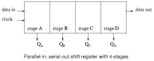
12.4. Serial-in, parallel-out shift registerA serial-in/parallel-out shift register is similar to the serial-in/ serial-out shift register in that it shifts data into internal storage elements and shifts data out at the serial-out, data-out, pin. It is different in that it makes all the internal stages available as outputs. Therefore, a serial-in/parallel-out shift register converts data from serial format to parallel format. If four data bits are shifted in by four clock pulses via a single wire at data-in, below, the data becomes available simultaneously on the four Outputs QA to QD after the fourth clock pulse.
The practical application of the serial-in/parallel-out shift register is to convert data from serial format on a single wire to parallel format on multiple wires. Perhaps, we will illuminate four LEDs (Light Emitting Diodes) with the four outputs (QA QB QC QD ).
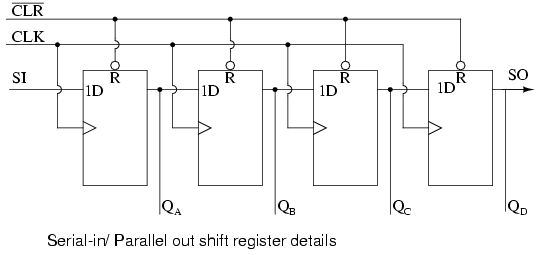
The above details of the serial-in/parallel-out shift register are fairly simple. It looks like a serial-in/ serial-out shift register with taps added to each stage output. Serial data shifts in at SI (Serial Input). After a number of clocks equal to the number of stages, the first data bit in appears at SO (QD) in the above figure. In general, there is no SO pin. The last stage (QD above) serves as SO and is cascaded to the next package if it exists. If a serial-in/parallel-out shift register is so similar to a serial-in/ serial-out shift register, why do manufacturers bother to offer both types? Why not just offer the serial-in/parallel-out shift register? They actually only offer the serial-in/parallel-out shift register, as long as it has no more than 8-bits. Note that serial-in/ serial-out shift registers come in gigger than 8-bit lengths of 18 to to 64-bits. It is not practical to offer a 64-bit serial-in/parallel-out shift register requiring that many output pins. See waveforms below for above shift register.
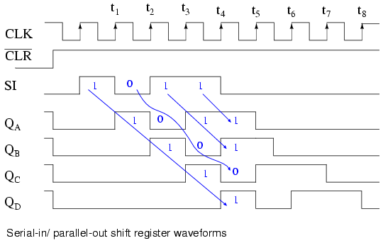
The shift register has been cleared prior to any data by CLR', an active low signal, which clears all type D Flip-Flops within the shift register. Note the serial data 1011 pattern presented at the SI input. This data is synchronized with the clock CLK. This would be the case if it is being shifted in from something like another shift register, for example, a parallel-in/ serial-out shift register (not shown here). On the first clock at t1, the data 1 at SI is shifted from D to Q of the first shift register stage. After t2 this first data bit is at QB. After t3 it is at QC. After t4 it is at QD. Four clock pulses have shifted the first data bit all the way to the last stage QD. The second data bit a 0 is at QC after the 4th clock. The third data bit a 1 is at QB. The fourth data bit another 1 is at QA. Thus, the serial data input pattern 1011 is contained in (QD QC QB QA). It is now available on the four outputs. It will available on the four outputs from just after clock t4 to just before t5. This parallel data must be used or stored between these two times, or it will be lost due to shifting out the QD stage on following clocks t5 to t8 as shown above. Serial-in/ parallel-out devicesLet's take a closer look at Serial-in/ parallel-out shift registers available as integrated circuits, courtesy of Texas Instruments. For complete device data sheets follow the links.
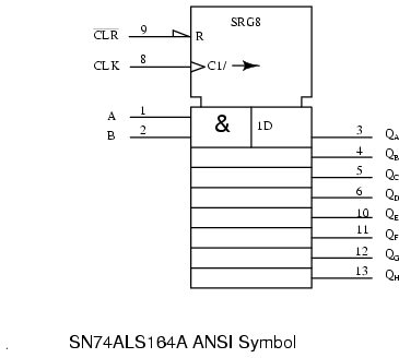
The 74ALS164A is almost identical to our prior diagram with the exception of the two serial inputs A and B. The unused input should be pulled high to enable the other input. We do not show all the stages above. However, all the outputs are shown on the ANSI symbol below, along with the pin numbers.
The CLK input to the control section of the above ANSI symbol has two internal functions C1, control of anything with a prefix of 1. This would be clocking in of data at 1D. The second function, the arrow after after the slash (/) is right (down) shifting of data within the shift register. The eight outputs are available to the right of the eight registers below the control section. The first stage is wider than the others to accommodate the A&B input.
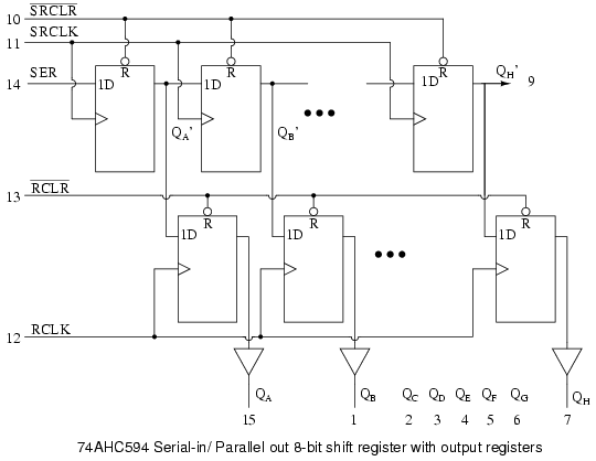
The above internal logic diagram is adapted from the TI (Texas Instruments) data sheet for the 74AHC594. The type "D" FFs in the top row comprise a serial-in/ parallel-out shift register. This section works like the previously described devices. The outputs (QA' QB' to QH' ) of the shift register half of the device feed the type "D" FFs in the lower half in parallel. QH' (pin 9) is shifted out to any optional cascaded device package. A single positive clock edge at RCLK will transfer the data from D to Q of the lower FFs. All 8-bits transfer in parallel to the output register (a collection of storage elements). The purpose of the output register is to maintain a constant data output while new data is being shifted into the upper shift register section. This is necessary if the outputs drive relays, valves, motors, solenoids, horns, or buzzers. This feature may not be necessary when driving LEDs as long as flicker during shifting is not a problem. Note that the 74AHC594 has separate clocks for the shift register (SRCLK) and the output register ( RCLK). Also, the shifter may be cleared by SRCLR and, the output register by RCLR. It desirable to put the outputs in a known state at power-on, in particular, if driving relays, motors, etc. The waveforms below illustrate shifting and latching of data.
The above waveforms show shifting of 4-bits of data into the first four stages of 74AHC594, then the parallel transfer to the output register. In actual fact, the 74AHC594 is an 8-bit shift register, and it would take 8-clocks to shift in 8-bits of data, which would be the normal mode of operation. However, the 4-bits we show saves space and adequately illustrates the operation. We clear the shift register half a clock prior to t0 with SRCLR'=0. SRCLR' must be released back high prior to shifting. Just prior to t0 the output register is cleared by RCLR'=0. It, too, is released ( RCLR'=1). Serial data 1011 is presented at the SI pin between clocks t0 and t4. It is shifted in by clocks t1 t2 t3 t4 appearing at internal shift stages QA' QB' QC' QD' . This data is present at these stages between t4 and t5. After t5 the desired data (1011) will be unavailable on these internal shifter stages. Between t4 and t5 we apply a positive going RCLK transferring data 1011 to register outputs QA QB QC QD . This data will be frozen here as more data (0s) shifts in during the succeeding SRCLKs (t5 to t8). There will not be a change in data here until another RCLK is applied.
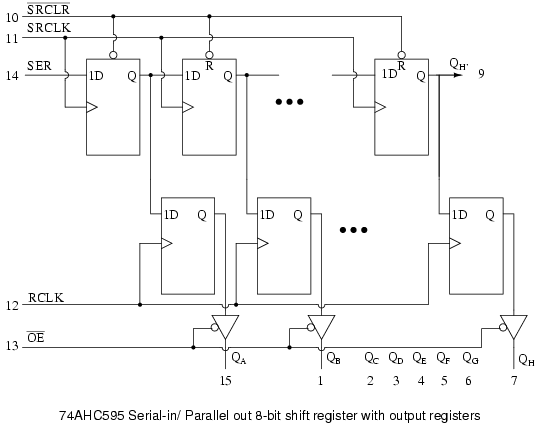
The 74AHC595 is identical to the '594 except that the RCLR' is replaced by an OE' enabling a tri-state buffer at the output of each of the eight output register bits. Though the output register cannot be cleared, the outputs may be disconnected by OE'=1. This would allow external pull-up or pull-down resistors to force any relay, solenoid, or valve drivers to a known state during a system power-up. Once the system is powered-up and, say, a microprocessor has shifted and latched data into the '595, the output enable could be asserted (OE'=0) to drive the relays, solenoids, and valves with valid data, but, not before that time.
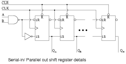
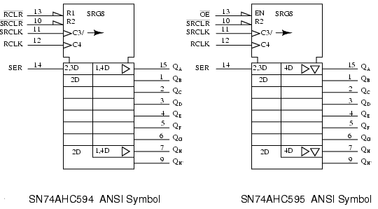
Above are the proposed ANSI symbols for these devices. C3 clocks data into the serial input (external SER) as indicate by the 3 prefix of 2,3D. The arrow after C3/ indicates shifting right (down) of the shift register, the 8-stages to the left of the '595symbol below the control section. The 2 prefix of 2,3D and 2D indicates that these stages can be reset by R2 (external SRCLR'). The 1 prefix of 1,4D on the '594 indicates that R1 (external RCLR') may reset the output register, which is to the right of the shift register section. The '595, which has an EN at external OE' cannot reset the output register. But, the EN enables tristate (inverted triangle) output buffers. The right pointing triangle of both the '594 and'595 indicates internal buffering. Both the '594 and'595 output registers are clocked by C4 as indicated by 4 of 1,4D and 4D respectively.
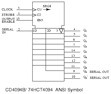
The CD4094B is a 3 to 15VDC capable latching shift register alternative to the previous 74AHC594 devices. CLOCK, C1, shifts data in at SERIAL IN as implied by the 1 prefix of 1D. It is also the clock of the right shifting shift register (left half of the symbol body) as indicated by the /(right-arrow) of C1/(arrow) at the CLOCK input. STROBE, C2 is the clock for the 8-bit output register to the right of the symbol body. The 2 of 2D indicates that C2 is the clock for the output register. The inverted triangle in the output latch indicates that the output is tristated, being enabled by EN3. The 3 preceding the inverted triangle and the 3 of EN3 are often omitted, as any enable (EN) is understood to control the tristate outputs. QS and QS' are non-latched outputs of the shift register stage. QS could be cascaded to SERIAL IN of a succeeding device. Practical applicationsA real-world application of the serial-in/ parallel-out shift register is to output data from a microprocessor to a remote panel indicator. Or, another remote output device which accepts serial format data.
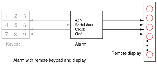
The figure "Alarm with remote key pad" is repeated here from the parallel-in/ serial-out section with the addition of the remote display. Thus, we can display, for example, the status of the alarm loops connected to the main alarm box. If the Alarm detects an open window, it can send serial data to the remote display to let us know. Both the keypad and the display would likely be contained within the same remote enclosure, separate from the main alarm box. However, we will only look at the display panel in this section. If the display were on the same board as the Alarm, we could just run eight wires to the eight LEDs along with two wires for power and ground. These eight wires are much less desirable on a long run to a remote panel. Using shift registers, we only need to run five wires- clock, serial data, a strobe, power, and ground. If the panel were just a few inches away from the main board, it might still be desirable to cut down on the number of wires in a connecting cable to improve reliability. Also, we sometimes use up most of the available pins on a microprocessor and need to use serial techniques to expand the number of outputs. Some integrated circuit output devices, such as Digital to Analog converters contain serial-in/ parallel-out shift registers to receive data from microprocessors. The techniques illustrated here are applicable to those parts.
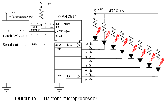
We have chosen the 74AHC594 serial-in/ parallel-out shift register with output register; though, it requires an extra pin, RCLK, to parallel load the shifted-in data to the output pins. This extra pin prevents the outputs from changing while data is shifting in. This is not much of a problem for LEDs. But, it would be a problem if driving relays, valves, motors, etc. Code executed within the microprocessor would start with 8-bits of data to be output. One bit would be output on the "Serial data out" pin, driving SER of the remote 74AHC594. Next, the microprocessor generates a low to high transition on "Shift clock", driving SRCLK of the '595 shift register. This positive clock shifts the data bit at SER from "D" to "Q" of the first shift register stage. This has no effect on the QA LED at this time because of the internal 8-bit output register between the shift register and the output pins (QA to QH). Finally, "Shift clock" is pulled back low by the microprocessor. This completes the shifting of one bit into the '595. The above procedure is repeated seven more times to complete the shifting of 8-bits of data from the microprocessor into the 74AHC594 serial-in/ parallel-out shift register. To transfer the 8-bits of data within the internal '595 shift register to the output requires that the microprocessor generate a low to high transition on RCLK, the output register clock. This applies new data to the LEDs. The RCLK needs to be pulled back low in anticipation of the next 8-bit transfer of data. The data present at the output of the '595 will remain until the process in the above two paragraphs is repeated for a new 8-bits of data. In particular, new data can be shifted into the '595 internal shift register without affecting the LEDs. The LEDs will only be updated with new data with the application of the RCLK rising edge. What if we need to drive more than eight LEDs? Simply cascade another 74AHC594 SER pin to the QH' of the existing shifter. Parallel the SRCLK and RCLK pins. The microprocessor would need to transfer 16-bits of data with 16-clocks before generating an RCLK feeding both devices. The discrete LED indicators, which we show, could be 7-segment LEDs. Though, there are LSI (Large Scale Integration) devices capable of driving several 7-segment digits. This device accepts data from a microprocessor in a serial format, driving more LED segments than it has pins by by multiplexing the LEDs. For example, see link below for MAX6955
|